Such as the automotive semiconductor market and the AI market, it is anticipated that demands of semiconductors will continue growing all over the world.
We UNIPULSE offer a huge variety of sensor products that can be used for various processes such as manufacturing, testing, servicing etc. of semiconductors.
From among them, we introduce "PS-IA", a non-contact capacitive displacement sensor in this issue.
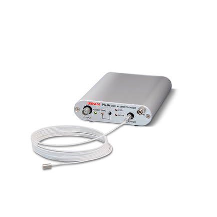
PS-IA is an ultra-precision non-contact displacement sensor that uses the capacitive method by the technology unique to UNIPULSE, and has achieved a high stability, a high resolution and the versatility.
It measures a distance between a metal (conducting body) and a measurement probe with the subnanometer resolution.
PS-IA: Recommended for such applications in semiconductor fabrication process!
● Thickness measurement of silicon wafer
Ideal for incorporating into machinery due to a probe with custom-made shape
● Flatness measurement of silicon wafer
The capacitive method is the most commonly used method for flatness measurement.
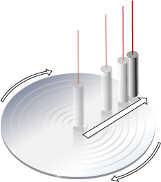
● Edge detection of silicon wafer
By scanning the surface of wafers in parallel at regular intervals with the measurement probe, edge positions of silicon wafers are detected.
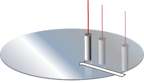
● Thickness measurement of insulating film or layer
For a thickness measurement of insulating film or layer in a gap between a measurement probe and GND.
Also ideal for thickness distribution of insulating film or layer by combining with positioning equipment. It's also useful for monitoring the thickness of unnecessary insulating film inside coating chambers, such as PVD or CVD equipment.
● Relative permittivity measurement of insulating film or layer
If a thickness is already known, it's also suitable for relative permittivity measurement of insulating film or layer.
● Feedback sensor of ultra-precision positioning stage
Ideal for positioning that requires nano level resolution, high precision and high stability
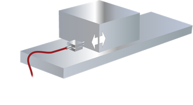
● Gap measurement of motor stator
As the capacitive method is not affected by electromagnetic induction, gap, position and vibration can be measured.
● Bubble measurement
By using the difference of a permittivity between liquid and bubble, bubble fraction in the liquid can be measured.
[Measurement image]

PS-IA: It is recommended because…
1. Conducting body can be detected with certainty
The capacitive method that PS-IA uses is less susceptible to surface roughness of a measured surface. With this method, a measurement is possible with even a patterned surface, which is difficult
to measure with an optical displacement sensor.
A silicone wafer can be detected too. It can be used for detection of a wafer edge as well.
2. Compatible with vacuum environment (*Custom-order)
Such as film-forming and edging etc., vacuum equipment is used for various processes. The probe of PS-IA can be made with less outgas generation for vacuum environment by a custom-order.
3. Compatible with high temperature environment (*Custom-order)
At an oxidation step of a wafer surface or a film-forming step of a thin film, the inside of manufacturing machinery becomes high temperature condition.
PS-IA can be compatible with high temperature environment by a custom-order.
4. Customizable probe shape (*Custom-order)
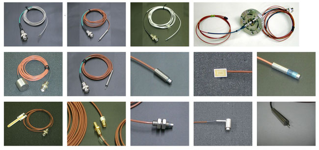
The sensor probe of PS-IA can be customized depending on applications. A low-profile sensor probe which is easy to incorporate into semiconductor machineries can be produced too. With a double-sided probe, tiny gaps can be measured and managed quantitatively. PS-IA can be used for a gap measurement and management of a flat-plate electrode.
Some examples of custom-made probes:
5. Stable position detection due to high stability & low noise
A stable position detection is possible with the high linearity of ±0.05% or less as well as the low noise of 0.002%FS (rms) or less.
6. Reliable Made-in-Japan quality
PS-IA is a Japanese-manufactured product with stable product quality.

